Monday, September 30, 2013

AUDIO LEVEL METER ELECTRONIC DIAGRAM


AUDIO LEVEL METER ELECTRONIC DIAGRAM

It consists of only few components. IC LM3915 converts the audio analog voltage and display it to the LED. Here is the schematic :

Parts list :


  •     Resistor R1 : 1k2
  •     Resistor variable R2 : 10k
  •     IC : LM3915
  •     LED indicator LED1-LED10 : LED 5mm
  •     12V power supply


Read More...

Saturday, September 28, 2013

Symmetric Noise Source

If a transistor junction operating in Zener breakdown is used as a noise source, the amplitude of the noise signal is asymmetric. This problem can be solved by using two transistors as two independent noise sources. One of these has a series resistor to earth, and the other has a series resistor to the supply line. Each of these noise sources produces an asymmetric noise voltage, with opposite asymmetry. If these two voltages are combined, the amplitude of the result will be symmetric. In the circuit diagram, T1 and T2 are the noise sources. The series resistors are R2 (to earth) and R4 (to the positive supply line).

The supply voltage for the noise sources has been made adjustable, to allow the noise generation of the transistors to be optimized. This is because the amount of noise produced depends on the power supply voltage. P1 and R1 provide an adjustable supply voltage between 8 and 12 V for the noise stage around T1, while P3 and R3 perform the same function for T2. C3 and C5 smooth these voltages. Since the amplitudes of the two noise sources will never be the same, it is necessary to take a weighted sum of the two signals. Consequently, P2 is included between the outputs of the noise sources as a sort of balance control.

Symmetric Noise Source circuit diagramSince the DC levels of the two noise sources are not the same, C4 is also included in the balance network. The weighted sum of the two signals is present on the wiper of P2, superimposed on the DC signal of noise source T1. This DC level is also used for the DC bias of the buffer stage T3. The buffer isolates the noise sources from whatever circuit is connected to the output. To adjust the circuit, connect an oscilloscope to the output. First, turn P2 all the way to the left. Now rotate P1 until a maximum noise signal is seen on the oscilloscope. Next, turn P2 all the way to the right, and then adjust P3 for the best noise signal. Finally, adjust P3 so that the noise signal looks symmetric. The circuit provides an output voltage of approximately 150mV pp. The current consumption is 2mA. The oscilloscope shows the asymmetric noise signal on channel 2, and the symmetric noise signal on channel 1.
Read More...

Thursday, September 26, 2013

Electronic Touch Switch

Mechanical contacts have the disadvantage that they wear out. That is why it is practical to use an electronic ‘touch switch’ in some situations. With such a touch switch the resistance of the human skin is used for the switching action. The schematic shows the design of a circuit that senses the resistance of the skin and converts it into a useful switching signal. The touch switch contacts can be made from two small metal plates, rivets, nails, etcetera, which are placed close together on a non-conducting surface. In this circuit a comparator of the type LM393 has been used. In the idle state there is, via R1, a voltage equal to the power supply voltage on the non-inverting input of IC1a. Because the inverting input of IC1a is set with R2 and D3 to D5 at the supply voltage minus 1.8 V, the open-collector output of IC1.a is, via R3, equal to the power supply voltage. This voltage is inverted by IC1.b. The voltage at the non-inverting input of IC1.b amounts to half the power supply voltage (through voltage divider R4 and R5) and is lower than the voltage on the inverting input.

Circuit diagram:

electronic-touch-switch-circuit-diagramw

Electronic Touch Switch Circuit Diagram

The output of IC1.b is therefore a ‘0’. If the two touch contacts are bridged with a finger, the voltage at the non-inverting input will become low enough to cause the comparator to toggle state. The moistness of the skin results in a resistance of 1 to 10 MR. If this circuit is used in the vicinity of equipment that’s connected to the mains, then it can be sufficient to touch only the upper contact to operate the switch, provided that the circuit has been earthed. The body then acts as an antenna which receives the 50 Hz (or 60 Hz) from the mains. This is enough to toggle IC1.a at the same 50 Hz. C1/R3 prevent this 50 Hz from reaching the input of IC1b and provide a useable ‘pulse’ of about 10 s at the output of IC1.b. Note that a fly walking across the touch switch conducts enough to generate a switching signal. So do not operate important things with this circuit (such as the heating system or the garage door). Do not make the wires between the touch contacts and the circuit too long to prevent picking up interference. The power supply voltage for the circuit is not very critical. Any regulated DC voltage in the range from 6 to 20 V can be used.

Author: Heino Peters - Copyright: Elektor Electronics Magazine

Read More...

Tuesday, September 24, 2013

Playback Amplifier For Cassette Deck

For some time now, there have been a number of tape cassette decks available at low prices from mail order businesses and electronics retailers. Such decks do not contain any electronics, of course. It is not easy to build a recording amplifier and the fairly complex magnetic biasing circuits, but a playback amplifier is not too difficult as the present one shows. The stereo circuits in the diagram, in conjunction with a suitable deck, form a good-quality cassette player. The distortion and frequency range (up to 23 kHz) are up to good standards. Moreover, the circuit can be built on a small board for incorporation with the deck in a suitable enclosure. Both terminals of coupling capacitor C1 are at ground potential when the amplifier is switched on.

Cassette Deck Playback Amplifier Circuit DiagramBecause of the symmetrical ±12 V supply lines, the capacitor will not be charged. If a single supply is used, the initial surge when the capacitor is being charged causes a loud click in the loudspeaker and, worse, magnetizes the tape. The playback head provides an audio signal at a level of 200–500 mV. The two amplifiers raise this to line level, not linearly, but in accordance with the RIAA equalization characteristic for tape recorders. Broadly speaking, this characteristic divides the frequency range into three bands:
  • Up to 50 Hz, corresponding to a time constant of 3.18 ms, the signal is highly and linearly amplified.
  • Between 50 Hz and 1.326 kHz, corresponding to a time constant of 120 µs, for normal tape, or 2.274 kHz, corresponding to a time constant of 70 µs, for chromium dioxide tape, the signal is amplified at a steadily decreasing rate.
  • Above 1.326 kHz or 2.274 kHz, as the case may be, the signal is slightly and linearly amplified. This characteristic is determined entirely by A1 (A1’). To make the amplifier suitable for use with chromium dioxide tape, add a double-pole switch (for stereo) to connect a 2.2 kΩ resistor in parallel with R3 (R3’). The output of A1 (A1’) is applied to a passive high-pass rumble filter, C3-R5 (C3’-R5’) with a very low cut-off frequency of 7 Hz. The components of this filter have exactly the same value as the input filter, C1-R1 (C1’-R1’). The second stage, A2 (A2’) amplifies the signal ´100, that is, to line level (1V r.m.s.).
Read More...

Sunday, September 22, 2013

CHALLENGES DESIGN OF SWITCHING LED ELECTRONIC DIAGRAM


CHALLENGES DESIGN OF SWITCHING LED ELECTRONIC DIAGRAM

The LED WEBENCH® online design environment predicts and simulates the response of an LED to constant current while taking into account several potential design parameters that are new to designers of traditional switching regulators.
Read More...

Friday, September 20, 2013

2000 Chevrolet Chevy Blazer Wiring Diagram

2000 Chevrolet Chevy Blazer Wiring Diagram
(click for full size image)

The Part of 2000 Chevrolet Chevy Blazer Wiring Diagram: power distribution schematic, fuel pump relay control, fuel pump and sender, splice pack, fuel pump prime connector, ground distribution svhematic, underhood fuse block, vehicle control module, fuel pump relay control..
Read More...

Wednesday, September 11, 2013

Mains sockets switched automatically by a Control Socket, Up to 1000W switched power

This circuit consists of a Trailing Socket (also called Extension or Distribution Socket) or similar device where two, three or more sockets (depending on the box dimensions and on constructors needs) will be powered only when a current flows in the Control Socket. For example: if an electric drill is connected to the Control Socket, the Switched Sockets will be powered each time the electric drill is running. In this case, a lamp could be connected to a Switched Socket and will illuminate when the drill is operating.

Another example: a desk lamp could be connected to the Control Socket and a PC, a Monitor and a Printer could be connected to the Switched Sockets and will be running after the lamp is switched on. Switching off the lamp, all the above mentioned appliances will be automatically switched off. A further application is the control of a High Fidelity chain, plugging the Power Amplifier in the Control Socket and - for example - CD Player, Tape Recorder, and Tuner in the Switched Sockets.

Usually, trailing sockets are placed to the rear of the appliances, often in places not easily reachable, so, even if the socket has a switch, it is much easier to switch on and off the High Fidelity chain from the main amplifier itself. The same consideration is valid for computer-monitor-printer chains etc. Nevertheless, in this case, the use of a table lamp plugged in the Control Socket is almost mandatory, as explained below. In fact, this very sensitive circuit works fine when appliances having full breaking switches like lamps, drills, most power amplifiers, old radios, old TV sets, fans, almost all electrical household appliances etc. are plugged in the Control Socket.

This is because these devices have a switch that fully excludes the internal circuitry from the mains. Unfortunately, in modern devices like computers, monitors, CD players, recent radios and TV sets (usually powered by means of internal "switching" supplies), the power switch does not completely isolate the internal circuitry from the mains, as transient suppressors and other components remain on circuit. This causes a very small current to flow across the sensing circuitry, but sufficient to trigger the output Triac.

Therefore, the switched devices will remain always on, no matter if the control appliance is on or off. This could also happen when devices connected to the mains by means of plug-in power supply adapters are used as control appliances, due to their lack of a mains switch. In spite of this restriction, the circuit can be still useful, due to the high number and variety of devices allowing impeccable performance when they are plugged in the Control Socket.


smart trailing socket circuit schematic
Parts:

R1,R2_________100R 1/2W Resistors
C1____________100nF 630V Polyester Capacitor
D1 to D6_____1N5408 1000V 3A Diodes (See Notes)
D7__________TIC225M 600V 8A Sensitive Gate Triac (See Notes)
A commercial trailing socket to be modified or a self-made box with several sockets.

Circuit operation:

Six back-to-back power diodes are connected in series to the Control Socket. The current drawn by the device plugged into this socket when in the on state, flowing through the diode chain, causes a voltage drop of about 2V. This voltage, limited by R1, drives the Gate of the Triac D7 which, in turn, will switch the output sockets. C1 and R2 form a so called "Snubber network", helping to eliminate switching transients generated by inductive loads.

Notes:
  • The circuit is sufficiently small to be embedded into some types of commercial trailing sockets, or a box with a number of sockets can be made at will.
  • The diode types suggested in the Parts List for D1 to D6 will allow an appliance of up to about 500W power to be plugged in the Control Socket. Use BY550-800 diodes for up to 800 - 1000W.
  • For less demanding appliances, 1N4007 diodes will allow up to 200W power.
  • The Triac type suggested in the Parts List for D7 will allow a total power available to the Switched Sockets of more than 1000W. If you intend to drive loads of more than 500W total, please use a suitable heatsink.
  • Wanting to drive less powerful loads, you can use for D7 a TIC216M (up to 800 - 1000W) or a TIC206M (up to 500 - 600W).
  • Warning! The device is connected to 230Vac mains, so some parts in the circuit board are subjected to lethal potential! Avoid touching the circuit when the mains cord is plugged in!
Read More...

Tuesday, September 3, 2013

Wireles Temperature Monitor Has Data Logging Capabilities

You can use a local temperature sensor and an ASK (amplitude-shift-keying) transmitter/receiver pair to design a simple wireless temperature-monitoring system with data-logging capabilities. A microcontroller processes and displays the temperature reading to the user. The microcontroller’s onboard UART (universal asynchronous receiver/transmitter) also allows for data-logging applications.
Wireless Temperature Monitor
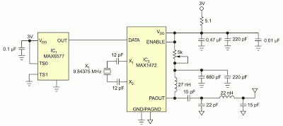
 Figure 1. The MaX6577 temperature sensor and 315-MHz MaX1472 aSk transmitter form a wireless temperature-monitoring system.

Local-temperature sensor IC1 detects the ambient temperature at the device (Figure 1). The output of IC1 is a square wave with a frequency proportional to temperature in kelvins. ASK transmitter IC2 modulates the signal onto the carrier frequency of 315 MHz. You measure the output signal’s frequency with a frequency counter. The configured scalar multiplier is 1K/Hz when the TS1 pin connects to ground and the TS0 pin connects to VDD. This scalar multiplier is configurable with pins TS1 and TS0. ASK receiver IC3 demodulates the signal at the corresponding carrier frequency (Figure 2).
 
Circuit Diagram
Figure 2. An ASK receiver with a microcontroller processes and displays temperature data.

Comparator IC4 connects to IC3’s RSSI (received-signal-strength indicator) with an internal peak detector. The external RC follows the peak power of the received signal and compares it with a predetermined, resistor-voltage-divider-generated voltage level. Lab experiments show that a threshold of approximately 1.57V generates a valid output on the data-out pin without receiving false readings. Adjust this threshold to the proper level for optimal performance. The comparator’s output is low when the received signal is weak or invalid and high when the received signal is adequate.

Microcontroller IC5 then measures and displays the value of the signal frequency using its integrated timer/counters and LCD-driver peripherals. A counter tracks the number of rising-edge transitions on the input temperature signal, and a timer tracks the elapsed time. After the timer’s 1-sec period elapses, an interrupt occurs. At that moment, the circuit reads the counter value, converts it to Celsius, and displays it on the LCD. The counter then resets to zero to restart the process. The timer automatically reloads once the timer interrupt occurs. UART0 also outputs the resulting temperature. A handheld frequency counter verifies the temperature reading.

The microcontroller monitors the signal power through P6.0, a general-purpose input pin. When the input is logic low, the LCD and UART output “no RF” to alert users of possible transmitter issues when the transmitter and receiver are too far apart from each other. The LCD connection follows the design in the IC’s evaluation kit (Figure 3). Using a look-up table in the data segment of the assembly code enables you to preserve the internal mapping of the display’s A through G segments. This preservation ensures that the display enables the correct segments. Using an RS-232 level converter, the UART output sends data to a data-logging device, such as a computer.

Kit

Figure 3. Maxim MAXQ2000-KIT Evaluation Kit.

Use the MAX-IDE assembler software to program the device during assembly. The MAXQJTAG board operates with the MAX-IDE to load the code onto the device. You can download the project files here. This design provides for a 1-sec temperature-refresh rate in 1°C increments, which is within the accuracy of IC1.

Downloads


Source Code (MAX-IDE assembler software) - download

MAXQ2000-KIT Evaluation Kit user manual and schematic - download
Read More...

Sunday, September 1, 2013

Simple Short Wave Transmitter Circuit

Description 
This low-cost short-wave transmitter is tunable from 10 to 15 MHz with the help of ½J gang condenser VC1, which determines the carrier frequency of the transmitter in conjunction with inductor L1. The frequency trimming can be done with VC2. The carrier is amplified by transistor T4 and coupled to RF amplifier transistor T1 (BD677) through transformer X1*. The transmitter does not use any modulator transformer.
The audio output from condenser MIC is preamplified by transistor T3 (BC548). The audio output from T3 is further amplified by transistor T2 (BD139), which modulates the RF amplifier built around transistor T1 by varying the current through it in accordance with the audio signal’s amplitude. RFC1 is used to block the carrier RF signal from transistor T2 and the power supply. The modulated RF is coupled to the antenna via capacitor C9.
Circuit Diagram:
 For antenna, one can use a 0.5m long telescopic aerial. Details of RF choke, inductor L1 and coupling RFC1 is used to block the carrier RF signal from transistor T2 and the power supply. The modulated RF is coupled to the antenna via capacitor C9. For antenna, one can use a 0.5m long telescopic aerial. Details of RF choke, inductor L1 and coupling transformer X1, we used a ready made short-wave antenna coil with tuning slug (Jawahar make), which worked satisfactorily. We tested the transmitter reception up to 75 metres and found good signal strength.

Read More...