Saturday, January 11, 2014

Variable Power Supply Using LM723

Using LM723 regulator can be designed a very simple variable power supply circuit which can provide a maximum current up to 2A and a variable voltage between 2 and 25 volts.This 25v variable power supply is designed using a LM723 regulator and a few common electronic components.Input voltage must be between 28 and 37 volts. Mj3000 transistor must be mounted on a radiator for heat dissipation.

LM723 Variable Power Supply Circuit diagram


Read More...

Friday, January 10, 2014

High Current Power Supply

Since my page was first posted, I have received a number of emails asking about a high current power supply. I looked around, but couldnt find one that was suitable. So, I designed this. It is a linear supply, which might have a few of you rolling your eyes, but it takes very few parts, is simple to build and can supply huge currents

High Current Power Supply Circuit diagram :

High Current Power Supply-Circuit diagram

Parts Table :

Part Total Qty Description
R1 1 680 Ohm 1/4 Watt Resistor
C1 1 20,000 - 50,000uF 20-40 Volt Capacitor   
C2, C3 2 100uF 50 Volt Capacitor
C4 1 0.1uF 50 Volt Capacitor
C5 1 0.01uF 50 Volt Capacitor
D1 1 Zener Diode (See Notes)   
Q1 1 2N3055 Or Other (See Notes)
T1 1 Transformer (See Notes)
BR1 1 Bridge Rectifier (See Notes)
S1 1 SPST 250 VAC 10 A Switch
MISC 1 Case, Line Cord, Heatsink For Q1, Binding Posts For Output

Notes :

  1. D1 should be rated at about one volt higher than then desired output of the supply. A half watt diode will do.
  2. Q1 can be a transistor similar to the 2N3055. I chose the 2N3055 for its availability and power handling (150 watts).
  3. T1 should be about 5 volts higher than the desired output of the supply, and rated for about one amp more of current. The voltage overhead is required by the regulator section. The extra current is to keep the transformer from over heating.
  4. The choice of BR1 will depend on the voltage and current of your transformer. The rectifier should be rated for 50 volts more than the transformer, and 5 amps more than the transformer.
  5. The value of R1 will be smaller when supplying high currents. Expiriment until you get what you need.
  6. Heatsink and fans are absolutely necessary!
Read More...

Mains Pulser

The pulser is intended to switch the mains voltage on and off at intervals between just under a second and up to 10 minutes. This is useful, for instance, when a mains-operated equipment is to be tested for long periods, or for periodic switching of machinery. Transformer Tr1, the bridge rectifier , and regulator IC1 provide a stable 12V supply rail for IC2 and the relay. The timer is arranged so that the period-determining capacitor can be charged and discharged independently. Four time ranges can be selected by selecting capacitors with the aid of jumpers. Short-circuiting positions 1 and 2 gives the longest time, and short-circuiting none the shortest.

Mains Pulser Circuit diagram:


In the latter case, the 10µF capacitor at pins 2 and 6 of the timer IC determines the time with the relevant resistors. The value of this capacitor may be chosen slightly lower. The two preset potentiometers enable the on and off periods to be set. The 1k resistor in series with one of the presets determines the minimum discharge time. The timer IC switches a relay whose double-pole contacts switch the mains voltage. The LEDs indicate whether the mains voltage is switched through (red) or not (green). The 100mA slow fuse protects the mains transformer and low-voltage circuit. The 4 A medium slow fuse protects the relay against overload.

Source :   http://www.ecircuitslab.com/2011/05/mains-pulser.html
Read More...

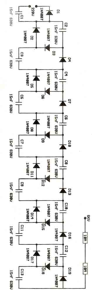
Build a Room Ioniser Circuit Diagram

This is a voltage multiplier circuit acting as an Room Ioniser Circuit Diagram. Its calculated to feed 220V from mains and the output is about 6KV. Caution should take with the circuit as can be dangerous due to mains. You can place a needle at the output 3cm long. Even you disconnect from mains, capacitors can be dangerous so make sure to discharge them by shorting their pins before you touch the circuit with hands.

Room Ioniser Circuit Diagram

Build a Room Ioniser Circuit Diagram
 
Read More...

Thursday, December 26, 2013

High Voltage Generator

This high voltage generator was designed  with the aim of testing the electrical break-down protection used on the railways. These  protection measures are used to ensure that  any external metal parts will never be at a  high voltage. If that were about to happen,  a very large current would flow (in the order  of kilo-amps), which causes the protection  to operate, creating a short circuit to ground effectively earthing the metal parts. This hap-pens when, for example, a lightning strike hits  the overhead line (or their supports) on the  railways.
This generator generates a high voltage of  1,000 V, but with an output current that is limited to few milliamps. This permits the electrical breakdown protection to be tested with-out it going into a short circuit state. The circuit uses common parts throughout: a  TL494 pulse-width modulator, several FETs or  bipolar switching transistors, a simple 1.4 VA  mains transformer and a discrete voltage multiplier. P1 is used to set the maximum current  and P2 sets the output voltage.

High Voltage Generator Circuit Diagram

High Voltage Generator-Circuit Diagram

The use of a voltage multiplier has the advantage that the working voltage of the smoothing capacitors can be lower, which makes them easier to obtain. The TL494 was chosen  because it can still operate at a voltage of  about 7 V, which means it can keep on working even when the batteries are nearly empty.  The power is provided by six C-type batteries, which keeps the total weight at a reason-able level.

The 2x4 V secondary of AC power transformer  (Tr1) is used back to front. It does mean that  the 4 V winding has double the rated voltage  across it, but that is acceptable because the  frequency is a lot higher (several kilo-Hertz)  than the 50 Hz (60 Hz) the transformer is  designed for. The final version also includes a display of the  output voltage so that the breakdown volt-age can be read.

From a historical perspective there follows a  bit of background information. In the past a different system was worked  out. Every high-voltage support post has a  protection system, and it isn’t clear when  the protection had operated and went into  a short-circuit state due to a large current  discharge.

Since very large currents were involved, a certain Mr. Van Ark figured out a solution for this.  He used a glass tube filled with a liquid containing a red pigment and a metal ball. When  a large current discharge occurred the metal  ball shot up due to the strong magnetic field,  which caused the pigment to mix with the liquid. This could be seen for a good 24 hours after the event. After a thunder storm it was  easy to see where a discharge current took  place: one only had to walk past the tubes  and have a good look at them.

Unfortunately, things didn’t work out as  expected. Since it often took a very long  time before a discharge occurred, the pigment settled down too much. When a dis-charge finally did occur the pigment no  longer mixed with the liquid and nothing was  visible. This system was therefore sidelined,  but it found its place in the (railway) history  books as the ‘balls of Van Ark’.
Author : By Jac Hettema – Copyright : Elektor

Source:  http://www.ecircuitslab.com/2012/03/high-voltage-generator.html
Read More...

Tuesday, December 24, 2013

Three Phase Appliance Protector

    Many of our costly appliances require three-phase AC supply for operation. Failure of any of the phases makes the appliance prone to erratic functioning and may even lead to failure. Hence it is of paramount importance to monitor the availability of the three-phase supply and switch off the appliance in the event of failure of one or two phases. The power to the appliance should resume with the availability of all phases of the supply with certain time delay in order to avoid surges and momentary fluctuations.


    The complete circuit of a three phase appliance protector is described here. It requires three-phase supply, three 12V relays and a timer IC NE555 along with 230V coil contactor havingfour poles. Relays RL1 and RL2 act as a sensing devices for phases Y and B, respectively. These relays are connected such that each acts as an enabling device for the subsequent relay. Therefore the combination of the relays forms a logical AND gate connected serially.

    The availability of phase R energises relay RL1 and its normally opened (N/O) contacts close to connect phase Y to the input of transformer X2. The availability of phase Y energises relay RL2 and its N/O contacts close to connect phase B to the input of transformer X3, thus applying a triggering input to timer IC NE555 (IC1).

    Therefore the delay timer built around NE555 triggers only when all the phases (R, Y and B) are available. It provides a delay of approximately four seconds, which energises relay RL3 and its N/O contact closes to connect the line to the energizing coil of four-pole contactor relay RL4. Contactor RL4 closes to ensure the availability of the three-phase supply to the appliance.

    The rating of contactor RL4 can be selected according to the full-load current rating of the appliances. Here the contact current rating of the four-pole contactor is up to 32A. The availability of phases R, Y and B is monitored by appropriate LEDs connected across the secondary windings of transformers X1, X2 and X3, respectively. Hence this circuit does not require a separate indicator lamp for monitoring the availability of the three phases. When phase R is available, LED1 glows. When phase Y is available, LED2 glows. When phase B is available, LED3 glows.

     The main advantage of this protector circuit is that it protects three-phase appliances from failure of any of the phases by disconnecting the power supply through the contactor and automatically restores the three-phase supply to the appliance (with reasonable time delay) when all the phases are available.
    Assemble the circuit on a general-purpose PCB and enclose in a cabinet with the relays and contactor mounted on the backside of cabinet. Connect the appliance through external wires.

    Caution:  To avoid the risk of electric shock, ensure that AC mains is disconnected during assembly of the circuit and double check everything before connecting your circuit to the mains.
Read More...

Sunday, December 22, 2013

Motional Feed Back Amplifier

This concept has appeared long back in Practical Electronics a UK based Magazine. Based on this concept I designed this circuit during 1981 to 1986 with lots of field trials and modifications, the design was frozen in 1986. I have assembled so many amplifiers for me and for my friends based on this design with various power levels. They are still kicking in so many houses. This concept can be applied to any existing amplifier also. You must listen to believe the crystal clear thumping bass response. crystal clear mid and hi frequencies. Good transient response with very low distortion. Hope you guys  will enjoy the reproduction of this amplifier.

In the art of audio sound reproduction it is well-known that the dynamic loudspeaker is more nonlinear and generates more distortion than all the other system components combined. This is particularly true at low frequencies which require large cone excursions where the stiffness of both the inner spider and the outer surround increases rapidly as the cone approaches its peak displacement, resulting in a nonlinear suspension compliance generating high distortion.

For example, in a typical high fidelity sound system at a frequency of about 35 Hz the total harmonic distortion of the amplifier might be of the order of 0.01%, whereas the distortion of the loudspeaker might range from about 3.0% to about 50.0%, depending upon the loudness. If this cone motion can be sensed and given as a feed back to the earlier stage of the amplifier, this distortion can be reduced dramatically.

Circuit diagram:

motional-feed-back-amplifier-circuit Diagram 

Motional Feed Back Amplifier Circuit Diagram

Motional Feedback (MFB) was a speaker system developed in the early 1970s by Philips Holland. It introduced a feedback system to the woofers of HiFi loudspeakers, enabling them to achieve a more extended low frequency response in a relatively small enclosure. The key benefits are a very controlled bass response. Any distortion induced by the enclosure or the woofer itself is immediately corrected by the feedback. These hand-built speakers were sounding very good and were quite expensive.

As a different approach, instead of using the cone movement, the current flow through the voice can be sensed (the current is proportional to cone movement) and can be used as a cone movement feedback. This novel idea is used in this amplifier design (I don’t claim any originality; this idea has appeared in Practical Electronics UK Magazine – long back – They might have even patented it).the amplifier used here is a standard Philips audio application circuit, with a specification of 40 Watt RMS @ < 0.06% Total Harmonic Distortion into 8 ohms impedance speaker and having a frequency response from 20Hz to 100 KHz, suitably modified for our application.

Powersupply Circuit:

power-supply-for-motional-feed-back

Motional Feed Back Amplifier Powersupply Circuit Diagram

The amplifier is a conventional class B directly coupled quasi complimentary out put stage, operating with single 56Volt supply (no need for a regulated or dual power supply). BC157 is the pre-driver and half supply stabilizer. BD 139 is the driver, a BD139 and a BD140 complimentary pair out put driver stage with 2N3055 as final out put stage. The speaker voice coil current is sensed through 0.47 ohms resistance connected from speaker one end to ground. This signal is given as negative fed back to previous stage through 470 ohms. The half supply at speaker coupling capacitor can be adjusted by varying the 39K resistance (if required you may fix a 100K pre set in the place of 39K and adjust for half supply with no in put signal at junction of both 0.47 ohms of out put transistors and speaker coupling capacitor).

The quiescent current through output transistors can be adjusted with 22 ohms in series with two bias diodes 1N4007. The value for 50mA quiescent current will lie between 15 to 33 ohms for a supply of 56volts. The amplifier can be protected with a simple 1.5Amp fast acting fuse in the positive power supply. the amplifier can be assembled on 40watt Philips amplifier application board or on any standard plain straight line board. All the three driver transistors require cooling clips. (Standard TO220 casing cooling fins). Out put transistors require a good quality extruded alloy heat sink with insulating mounting kit and with a smear of silicon conductive grease, for good conductance of heat.

Read More...

Friday, December 20, 2013

Bass Treble Tone Control

The LM1036 is a DC controlled tone (bass/treble), volume and balance circuit for stereo applications in car radio, TV and audio systems. An additional control input allows loudness compensation to be simply effected. Four control inputs provide control of the bass, treble, balance and volume functions through application of DC voltages from a remote control system or, alternatively, from four potentiometers which may be biased from a zener regulated supply provided on the circuit.

Bass Treble Tone Control Circuit diagram :


bass-treble-tone-control-circuit


Each tone response is defined by a single capacitor chosen to give the desired characteristic.

Features :
  • Wide supply voltage range, 9V to 16V
  • Large volume control range, 75 dB typical
  • Tone control, ±15 dB typical
  • Channel separation, 75 dB typical
  • Low distortion, 0.06% typical for an input level of 0.3 Vrms
  • High signal to noise, 80 dB typical for an input level of 0.3 Vrms
  • Few external components required
Note :

Vcc can be anything between 9V to 16V and the output capacitors are 10uF/25V electrolytic


Read More...

Wednesday, December 18, 2013

Step up Down DC DC Converter Circuit Diagram

Positive output step-up and step-down dc-dc converters have a common limitation in that neither can handle input voltages that are both greater than or less than the output. For example, when converting a 12-V sealed lead/acid battery to a regulated +12 V output, the battery voltage might vary from a high of 15 V down to 10 V. 

By using a MAX641 to drive separate P-and N-cbannel MOSFETs, both ends of the inductor are switched to allow noninverting buck/boost operation. A second advantage of the circuit over most boostonly designs is that the output goes to 0 V when shutdown is activated. Inefficiency is a drawback because two MOSFETs and two diodes increase the losses in the charge and discharge path of the inductor. The circuit delivers +12 V at 100 mA at 70 percent efficiency with an 8-V input.


Step up Down DC - DC Converter Circuit Diagram

Step up Down DC - DC Converter Circuit Diagram

Read More...

Thursday, October 10, 2013

Floating 9V Supply For DVM Modules

Most commercial DVM modules with an LCD readout are 9-V powered and based on an ICL7106 or similar A-D converter chip. These modules are typically used in laboratory power supplies and other test and measurement equipment where a drop-in solution needs to be found to realize a voltmeter readout. Particularly in power supply units, the LCD module will need to ‘float’ relative to the PSU supply rails, and this inevitably requires a separate 9-volt power supply. In some cases, batteries may be used but these have distinct advantages. The alternative, a 9-V converter effectively powered by the PSU and yet floating, is shown here.

Floating 9V Supply For DVM Modules Circuit Diagram
It is built from the ubiquitous TLC555, LMC555 or 7555) timer IC acting in astable multivibrator configuration producing a 70-kHz square wave fed into a simple rectifier. In essence, capacitors C5 and C6 afford the above mentioned electrical isolation between the PSU supply rails and the LCD module. The old, bipolar NE555 IC should not be used here because it presents a too heavy loads on the converter’s own supply voltage. Depending on the exact type and brand of the CMOS 555 you’re using, resistor R6 may need to be redimensioned a bit to ensure a supply voltage of about 10 volts at pins 8 and 4 of the chip. At an output voltage of 9.5 V, the maximum output current of the converter s about 1 mA.
Read More...

Tuesday, October 8, 2013

Automatic Switch For Voltage Converters

New applications for DC voltage converters, such as the ‘workhorse’ LT1070, arise every day. These converters can be adapted to nearly every imaginable ratio of input and output voltages. However, all of these circuits and devices have the same shortcoming, which is that they lack an on/off switch. Especially when they are used as a source of 6-V / 12-V power for a car radio, this is highly impractical. The circuit described here adds automatic load detection to the converter. For use in a car, the additional circuitry must be small and fit into a compact enclosure together with the converter.

Since the battery voltage and ambient temperature vary over wide ranges, a simple form of load detection must be used. Besides this, the voltage drop across the load sensing circuitry must naturally be as small as possible. This can be achieved by using ‘ultra-modern’ SiGe technology. The 6 V from the battery and the 12 V from the converter are combined in the MB R2545 dual diode. Consequently, a voltage of at least 6 V is always applied to the radio (for memory retention). If the radio is switched on, it draws a current from the 6-V battery, which may be around 100 mA.

This current produces a voltage across R1. If this voltage is 75 mV or greater, the AC128 germanium transistor starts conducting and charges electrolytic capacitor C1, which is connected to the gate of the BUZ10. The MOSFET energises RE1 and thus connects the supply voltage to the converter. As a result, 12-V power is connected to the radio. The resulting increased current causes the voltage drop across R1 to increase, which is undesirable, so a 10-A Schottky diode is connected in parallel. The total voltage drop is thus approximately 0.6 V. The RC network connected to the BUZ10 ensures that the transistor always remains switched on for at least several seconds, to prevent the circuit from ‘chattering’ with varying current consumption.

Automatic Switch Circuit Diagram For Voltage Converters
If the load is switched off, the AC128 cuts off, the electrolytic capacitor discharges and the relay again disconnects the voltage converter. The residual current consumption is so small that the circuit can also be connected ahead of the ignition switch. The Schottky diodes need only be rated for the necessary voltages and currents, and above all, they should have the lowest possible saturation voltage. The exact type is not critical. Two separate diodes can also be used. A small heat sink for the MBR diode won’t hurt, but this is normally not essential. Practically any type of PNP germanium transistor that is still available or on hand can be used (AC125, AC126 and AC128 work perfectly).

It may be necessary to modify the value of R1. In combination with the germanium transistor, R1 determines which level of current will be ignored (for memory retention) and which level of current will cause the converter to be switched on. With the component values shown in Figure 1, this level is between 10 mA and 25 mA. It is recommended to measure the quiescent current (at 6 V) and switch-on current of the load and then simulate the switching process using dummy load resistors. When selecting the 6-V relay, ensure that its contacts have an adequate current rating. The actual value can be significantly greater than the nominal output current. With a load of 5 A at 12 V and a converter efficiency of 70 percent, the current through the relay contacts rises to 14.3 A.
Read More...

Sunday, October 6, 2013

3V DC to 5V DC REGULATED POWER SUPPLY ELECTRONIC DIAGRAM


3V DC to 5V DC REGULATED POWER SUPPLY ELECTRONIC DIAGRAM

A 5V DC regulated output from 2 cells 3V DC batteries. The output current of the circuit is limited to 50mA. However, it still able to supply many microcontroller circuits. 3009 and 560R Resistor provide the 5V DC output, make up a voltage divider network.
Read More...

Friday, October 4, 2013

A Simple MD Catridge Preamplifier

Phonographs are gradually becoming a rarity. Most of them have had to yield to more advanced systems, such as CD players and recorders or (portable) MiniDisc player/recorders. This trend is recognized by manufacturers of audio installations, which means that the traditional phono input is missing on increasingly more systems. Hi-fi enthusiasts who want make digital versions of their existing collections of phonograph records on a CD or MD, discover that it is no longer possible to connect a phonograph to the system.

Circuit diagram :

A Simple MD Catridge Preamplifier Circuit daigram A Simple MD Catridge Preamplifier Circuit Diagram

However, with a limited amount of circuitry, it is possible to adapt the line input of a modern amplifier or recorder so that it can handle the low-level signals generated by the magnetodynamic cartridge of a phonograph. Of course, the circuit has to provide the well-known RIAA correction that must be used with these cartridges. The preamplifier shown here performs the job using only one opamp, four resistors and four capacitors. For a stereo version, you will naturally need two of everything. Any stabilized power supply that can deliver ±15V can be used as a power source.

Author : H. Steeman

Read More...

Wednesday, October 2, 2013

Optimised Semiconductor Noise Source

We have already published designs that use a transistor junction operating in Zener breakdown as a noise source. Anyone who has experimented with a reverse-biased transistor knows that the amplitude of the noise voltage generated in this manner is strongly dependent on the supply voltage. The variation between individual transistors is also rather large. An obvious solution is to use an adjustable supply voltage for the noise generator stage. A BC547B starts to break down at around 8V.

Optimized Semiconductor Noise SourceUsing P1 and R1, you can adjust the voltage across T1 and R2 between 8 and 12V. C3 decouples the reduced supply voltage. An impedance buffer in the form of T2 and R3 is added to the circuit, to prevent the connected load from affecting the noise source. This buffer is powered directly from the 12-V supply. To adjust this circuit, connect the output to an oscilloscope. Then adjust P1 to obtain the highest signal amplitude, combined with the best ‘shape’ of the noise signal. The output voltage is approximately 300mVpp, and the current consumption is around 2mA.
Read More...

Monday, September 30, 2013

AUDIO LEVEL METER ELECTRONIC DIAGRAM


AUDIO LEVEL METER ELECTRONIC DIAGRAM

It consists of only few components. IC LM3915 converts the audio analog voltage and display it to the LED. Here is the schematic :

Parts list :


  •     Resistor R1 : 1k2
  •     Resistor variable R2 : 10k
  •     IC : LM3915
  •     LED indicator LED1-LED10 : LED 5mm
  •     12V power supply


Read More...

Saturday, September 28, 2013

Symmetric Noise Source

If a transistor junction operating in Zener breakdown is used as a noise source, the amplitude of the noise signal is asymmetric. This problem can be solved by using two transistors as two independent noise sources. One of these has a series resistor to earth, and the other has a series resistor to the supply line. Each of these noise sources produces an asymmetric noise voltage, with opposite asymmetry. If these two voltages are combined, the amplitude of the result will be symmetric. In the circuit diagram, T1 and T2 are the noise sources. The series resistors are R2 (to earth) and R4 (to the positive supply line).

The supply voltage for the noise sources has been made adjustable, to allow the noise generation of the transistors to be optimized. This is because the amount of noise produced depends on the power supply voltage. P1 and R1 provide an adjustable supply voltage between 8 and 12 V for the noise stage around T1, while P3 and R3 perform the same function for T2. C3 and C5 smooth these voltages. Since the amplitudes of the two noise sources will never be the same, it is necessary to take a weighted sum of the two signals. Consequently, P2 is included between the outputs of the noise sources as a sort of balance control.

Symmetric Noise Source circuit diagramSince the DC levels of the two noise sources are not the same, C4 is also included in the balance network. The weighted sum of the two signals is present on the wiper of P2, superimposed on the DC signal of noise source T1. This DC level is also used for the DC bias of the buffer stage T3. The buffer isolates the noise sources from whatever circuit is connected to the output. To adjust the circuit, connect an oscilloscope to the output. First, turn P2 all the way to the left. Now rotate P1 until a maximum noise signal is seen on the oscilloscope. Next, turn P2 all the way to the right, and then adjust P3 for the best noise signal. Finally, adjust P3 so that the noise signal looks symmetric. The circuit provides an output voltage of approximately 150mV pp. The current consumption is 2mA. The oscilloscope shows the asymmetric noise signal on channel 2, and the symmetric noise signal on channel 1.
Read More...

Thursday, September 26, 2013

Electronic Touch Switch

Mechanical contacts have the disadvantage that they wear out. That is why it is practical to use an electronic ‘touch switch’ in some situations. With such a touch switch the resistance of the human skin is used for the switching action. The schematic shows the design of a circuit that senses the resistance of the skin and converts it into a useful switching signal. The touch switch contacts can be made from two small metal plates, rivets, nails, etcetera, which are placed close together on a non-conducting surface. In this circuit a comparator of the type LM393 has been used. In the idle state there is, via R1, a voltage equal to the power supply voltage on the non-inverting input of IC1a. Because the inverting input of IC1a is set with R2 and D3 to D5 at the supply voltage minus 1.8 V, the open-collector output of IC1.a is, via R3, equal to the power supply voltage. This voltage is inverted by IC1.b. The voltage at the non-inverting input of IC1.b amounts to half the power supply voltage (through voltage divider R4 and R5) and is lower than the voltage on the inverting input.

Circuit diagram:

electronic-touch-switch-circuit-diagramw

Electronic Touch Switch Circuit Diagram

The output of IC1.b is therefore a ‘0’. If the two touch contacts are bridged with a finger, the voltage at the non-inverting input will become low enough to cause the comparator to toggle state. The moistness of the skin results in a resistance of 1 to 10 MR. If this circuit is used in the vicinity of equipment that’s connected to the mains, then it can be sufficient to touch only the upper contact to operate the switch, provided that the circuit has been earthed. The body then acts as an antenna which receives the 50 Hz (or 60 Hz) from the mains. This is enough to toggle IC1.a at the same 50 Hz. C1/R3 prevent this 50 Hz from reaching the input of IC1b and provide a useable ‘pulse’ of about 10 s at the output of IC1.b. Note that a fly walking across the touch switch conducts enough to generate a switching signal. So do not operate important things with this circuit (such as the heating system or the garage door). Do not make the wires between the touch contacts and the circuit too long to prevent picking up interference. The power supply voltage for the circuit is not very critical. Any regulated DC voltage in the range from 6 to 20 V can be used.

Author: Heino Peters - Copyright: Elektor Electronics Magazine

Read More...

Tuesday, September 24, 2013

Playback Amplifier For Cassette Deck

For some time now, there have been a number of tape cassette decks available at low prices from mail order businesses and electronics retailers. Such decks do not contain any electronics, of course. It is not easy to build a recording amplifier and the fairly complex magnetic biasing circuits, but a playback amplifier is not too difficult as the present one shows. The stereo circuits in the diagram, in conjunction with a suitable deck, form a good-quality cassette player. The distortion and frequency range (up to 23 kHz) are up to good standards. Moreover, the circuit can be built on a small board for incorporation with the deck in a suitable enclosure. Both terminals of coupling capacitor C1 are at ground potential when the amplifier is switched on.

Cassette Deck Playback Amplifier Circuit DiagramBecause of the symmetrical ±12 V supply lines, the capacitor will not be charged. If a single supply is used, the initial surge when the capacitor is being charged causes a loud click in the loudspeaker and, worse, magnetizes the tape. The playback head provides an audio signal at a level of 200–500 mV. The two amplifiers raise this to line level, not linearly, but in accordance with the RIAA equalization characteristic for tape recorders. Broadly speaking, this characteristic divides the frequency range into three bands:
  • Up to 50 Hz, corresponding to a time constant of 3.18 ms, the signal is highly and linearly amplified.
  • Between 50 Hz and 1.326 kHz, corresponding to a time constant of 120 µs, for normal tape, or 2.274 kHz, corresponding to a time constant of 70 µs, for chromium dioxide tape, the signal is amplified at a steadily decreasing rate.
  • Above 1.326 kHz or 2.274 kHz, as the case may be, the signal is slightly and linearly amplified. This characteristic is determined entirely by A1 (A1’). To make the amplifier suitable for use with chromium dioxide tape, add a double-pole switch (for stereo) to connect a 2.2 kΩ resistor in parallel with R3 (R3’). The output of A1 (A1’) is applied to a passive high-pass rumble filter, C3-R5 (C3’-R5’) with a very low cut-off frequency of 7 Hz. The components of this filter have exactly the same value as the input filter, C1-R1 (C1’-R1’). The second stage, A2 (A2’) amplifies the signal ´100, that is, to line level (1V r.m.s.).
Read More...

Sunday, September 22, 2013

CHALLENGES DESIGN OF SWITCHING LED ELECTRONIC DIAGRAM


CHALLENGES DESIGN OF SWITCHING LED ELECTRONIC DIAGRAM

The LED WEBENCH® online design environment predicts and simulates the response of an LED to constant current while taking into account several potential design parameters that are new to designers of traditional switching regulators.
Read More...

Friday, September 20, 2013

2000 Chevrolet Chevy Blazer Wiring Diagram

2000 Chevrolet Chevy Blazer Wiring Diagram
(click for full size image)

The Part of 2000 Chevrolet Chevy Blazer Wiring Diagram: power distribution schematic, fuel pump relay control, fuel pump and sender, splice pack, fuel pump prime connector, ground distribution svhematic, underhood fuse block, vehicle control module, fuel pump relay control..
Read More...